Royalty-Free AI generated

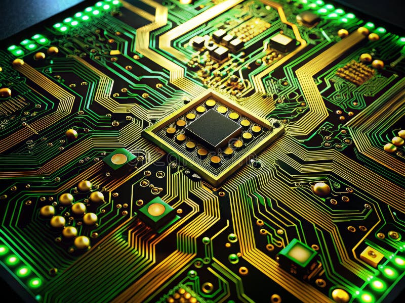
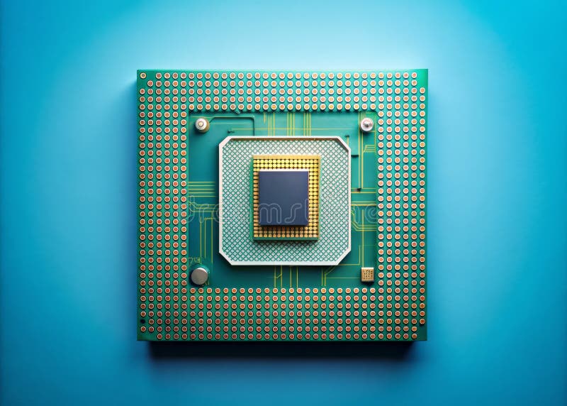
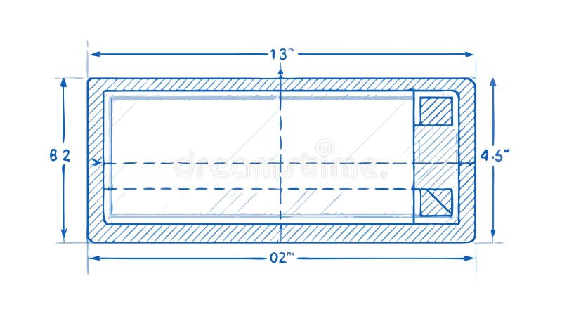
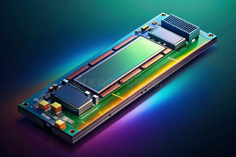
Comprehensive Technical Drawing of a Detailed Printed Circuit Board Design for Manufacturing. This detailed technical drawing showcases a meticulously crafted printed circuit board (PCB) pattern. The image provides a comprehensive view of the PCB layout, including component placement, copper traces, vias, and solder mask. It highlights critical aspects of printed circuit board design, such as surface mount and through-hole component arrangements. The technical drawing is essential for
- ?
$62.50USD
$150.00USD
$250.00USD
Size MAX
8192x4096px •
27.3" x 13.7" • @300dpi •
19.3MB • jpg
Author credit line
Image keywords
Related searches
More similar stock illustrations


More stock photos from Curie Duprat's portfolio