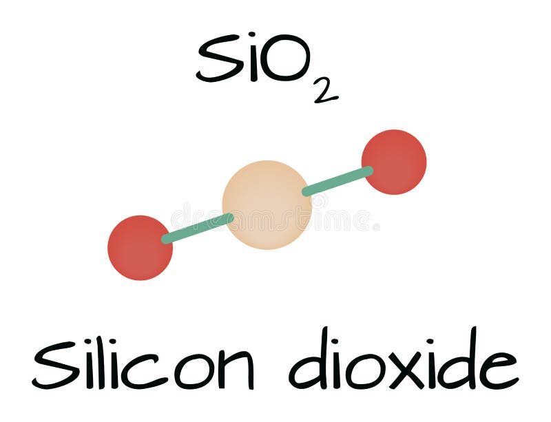
Free with trial Silicon dioxide, silica, SiO2, molecule model, chemical structure and formula. Commonly found in nature as quartz, a major constituent of sand, and a common fundamental constituent of glass. Vector. Silicon dioxide vectors Silicon dioxide, silica, SiO2, molecule model. Chemical structure and formula. Commonly found in nature as quartz, a major constituent of sand, and a common. Silicon dioxide, silica, SiO2, molecule model, chemical structure and formula. Commonly found in nature as quartz, a major constituent of sand, and a common fundamental constituent of glass. Vector.
Free with trial Molecule SiO2 Silicon dioxide. Isolated on white. Silicon dioxide vectors Molecule SiO2 Silicon dioxide. Isolated on white
Free with trial Molecule SiO2 Silicon dioxide. On white. Silicon dioxide vectors Molecule SiO2 Silicon dioxide. On white
Free with trial Vector bag or package of a granular and porous form of silica SiO2 e for the adsorption produced synthetically with high porosity which allows easy adsorption of water isolated on a white background. Desiccant hygroscopy substance. Silicon dioxide vectors Realistic illustration of silica gel. Two small white packages with spilled pile of balls. Amorphous and porous silicon dioxide. Vector bag or package of a. Vector bag or package of a granular and porous form of silica SiO2 e for the adsorption produced synthetically with high porosity which allows easy adsorption of water isolated on a white background. Desiccant hygroscopy substance.
Free with trial Thermal Oxidation: line art icon of the furnace process that converts the surface of a silicon wafer into silicon dioxide. Heating coils surround the chamber at roughly 800 to 1200 degrees Celsius, and oxygen molecules, or steam in wet oxidation, arrive at the front and back faces. Inside each insulating layer, small arrows trace the oxidant diffusing to the interface, where the reaction actually happens, so growth slows as the film thickens, as described by the Deal-Grove model. A dashed line records the original surface: around 44 percent of the finished thickness lies below it because substrate material is consumed, which separates this method from deposition. Grown oxide gives a near-perfect interface and is used for gate, pad, screen and field layers. Clean with no text, suited to microelectronics training, presentations and infographics. Part of the Semiconductor Manufacturing series of icons and process diagrams. Silicon dioxide vectors Thermal Oxidation silicon dioxide grown from a wafer's own silicon in a hot oxygen furnace, line icon. Thermal Oxidation: line art icon of the furnace process. Thermal Oxidation: line art icon of the furnace process that converts the surface of a silicon wafer into silicon dioxide. Heating coils surround the chamber at roughly 800 to 1200 degrees Celsius, and oxygen molecules, or steam in wet oxidation, arrive at the front and back faces. Inside each insulating layer, small arrows trace the oxidant diffusing to the interface, where the reaction actually happens, so growth slows as the film thickens, as described by the Deal-Grove model. A dashed line records the original surface: around 44 percent of the finished thickness lies below it because substrate material is consumed, which separates this method from deposition. Grown oxide gives a near-perfect interface and is used for gate, pad, screen and field layers. Clean with no text, suited to microelectronics training, presentations and infographics. Part of the Semiconductor Manufacturing series of icons and process diagrams.
Free with trial Hard Mask: line art icon of the durable intermediate film that guards a wafer during deep plasma etching. Modern photoresist is too thin and soft to survive a long reactive ion etch, so its pattern is first copied into an inorganic layer such as silicon nitride, silicon dioxide, titanium nitride or amorphous carbon. That film then does the protecting. Here a uniform ion shower falls across the surface: arrows landing on the hatched caps stop at their top face, while those passing through the gaps drive straight down, carving vertical trenches with high aspect ratios into one continuous target layer. Each cap sits flush with the trench walls below, showing faithful pattern transfer. After etching, the mask is usually stripped or kept for later steps. Schematic, not to scale. Clean with no text, suited to microelectronics, nanofabrication, cleanroom training, presentations and infographics. Part of the Semiconductor Manufacturing series of icons and process diagrams. Silicon dioxide vectors Hard Mask : an etch-resistant layer stops plasma ions while open areas etch into deep trenches, line icon. Hard Mask: line art icon of the durable intermediate. Hard Mask: line art icon of the durable intermediate film that guards a wafer during deep plasma etching. Modern photoresist is too thin and soft to survive a long reactive ion etch, so its pattern is first copied into an inorganic layer such as silicon nitride, silicon dioxide, titanium nitride or amorphous carbon. That film then does the protecting. Here a uniform ion shower falls across the surface: arrows landing on the hatched caps stop at their top face, while those passing through the gaps drive straight down, carving vertical trenches with high aspect ratios into one continuous target layer. Each cap sits flush with the trench walls below, showing faithful pattern transfer. After etching, the mask is usually stripped or kept for later steps. Schematic, not to scale. Clean with no text, suited to microelectronics, nanofabrication, cleanroom training, presentations and infographics. Part of the Semiconductor Manufacturing series of icons and process diagrams.
Free with trial Black and white of quartz crystals characterized by elongated, geometric shapes. The crystals showcase sharp, angular edges with parallel lines accentuating their contours. The arrangement suggests a cluster emanating from a common base, typical of natural crystal formations. The monochrome style emphasizes contrast and gives the image a bold, graphic quality. Quartz is a common mineral, silicon dioxide (SiO ), noted for its hardness and hexagonal crystal system. Silicon dioxide vectors Black and white of quartz crystals characterized by elongated, geometric shapes. The crystals showcase sharp, angular edges with parallel lines accentuating
Free with trial Chemical compound set featuring sulfuric ethanol monoxide dioxide bicarbonate ozone oxygen water peroxide methane ammonia benzene chloride carbonate propane formulas. Silicon dioxide vectors Chemical compound set featuring sulfuric. Ethanol monoxide dioxide bicarbonate ozone oxygen water peroxide methane ammonia benzene chloride carbonate propane
Free with trial Chemical compound set featuring sulfuric ethanol monoxide dioxide bicarbonate ozone oxygen water peroxide methane ammonia benzene chloride carbonate propane formulas. Silicon dioxide vectors Chemical compound set featuring sulfuric. Ethanol monoxide dioxide bicarbonate ozone oxygen water peroxide methane ammonia benzene chloride carbonate propane
Free with trial Chemical compound set featuring sulfuric ethanol monoxide dioxide bicarbonate ozone oxygen water peroxide methane ammonia benzene chloride carbonate propane formulas. Silicon dioxide vectors Chemical compound set featuring sulfuric. Ethanol monoxide dioxide bicarbonate ozone oxygen water peroxide methane ammonia benzene chloride carbonate propane
Free with trial Etch Selectivity: line art icon of the property that lets a fab clear one film while sparing the material next to it. Two blocks share a substrate and receive an identical shower of ions. On the left, the arrows travel down into empty space, and a dashed outline marks where the target stood before most of it was cleared. On the right, a dotted block keeps its full height, its top surface untouched. Selectivity is expressed as a ratio of etch rates, for example 20:1, meaning twenty nanometres of target vanish for every nanometre lost from the neighbour. Chemistry provides it: gases are chosen to form volatile products with silicon, oxide or nitride but not with the protected layer, then ion energy and gas mix are tuned. A high ratio safeguards thin gate oxides, masks and stop layers. Schematic, not to scale. Clean with no text, suited to microelectronics, training, presentations and infographics. Part of the Semiconductor Manufacturing series of icons and process diagrams. Silicon dioxide vectors Etch Selectivity : same ions hit two materials the target etches deep, the neighbour stays intact, line icon. Etch Selectivity: line art icon of the property. Etch Selectivity: line art icon of the property that lets a fab clear one film while sparing the material next to it. Two blocks share a substrate and receive an identical shower of ions. On the left, the arrows travel down into empty space, and a dashed outline marks where the target stood before most of it was cleared. On the right, a dotted block keeps its full height, its top surface untouched. Selectivity is expressed as a ratio of etch rates, for example 20:1, meaning twenty nanometres of target vanish for every nanometre lost from the neighbour. Chemistry provides it: gases are chosen to form volatile products with silicon, oxide or nitride but not with the protected layer, then ion energy and gas mix are tuned. A high ratio safeguards thin gate oxides, masks and stop layers. Schematic, not to scale. Clean with no text, suited to microelectronics, training, presentations and infographics. Part of the Semiconductor Manufacturing series of icons and process diagrams.
Free with trial A detailed close-up of a smoky quartz crystal cluster featuring multiple sharp, translucent points against a pure white background. This stunning macro representation of mineral structure and clarity was Rendered by Ai. Silicon dioxide vectors Smoky Quartz Crystal Cluster Macro Shot. A detailed close-up of a smoky quartz crystal cluster featuring multiple sharp, translucent points against a pure white. A detailed close-up of a smoky quartz crystal cluster featuring multiple sharp, translucent points against a pure white background. This stunning macro representation of mineral structure and clarity was Rendered by Ai
Free with trial Flower scientific anatomy icons featuring detailed botanical structures plant education diagrams floral biology resources and academic learning materials. Silicon dioxide vectors Flower Scientific Anatomy Icons for Botany Learning and Plant Research. Flower scientific anatomy icons featuring detailed botanical structures plant education. Flower scientific anatomy icons featuring detailed botanical structures plant education diagrams floral biology resources and academic learning materials
Free with trial Silica chemical icon. Beige button symbol. Mineral compound Vector. Science formula sign. EPS 10. Silicon dioxide vectors Silica chemical icon. Beige button symbol. Mineral compound Vector. Science formula sign. EPS 10
Free with trial Line icon of chemical vapour deposition (CVD), the process that grows thin films from reactive gases. Precursor gas enters a chamber through an inlet and a perforated showerhead, then drifts down as two-atom molecules toward a wafer resting on a coil-heated platen. At the hot surface, molecules break apart: atoms sink into the growing layer while by-product fragments leave through exhaust ports on both sides. Schematic, not to scale. Part of the Semiconductor Manufacturing series. Silicon dioxide vectors Chemical Vapour Deposition (CVD). Precursor gas reacts on a heated wafer to build a thin film, line icon. Line icon of chemical vapour deposition (CVD), the. Line icon of chemical vapour deposition (CVD), the process that grows thin films from reactive gases. Precursor gas enters a chamber through an inlet and a perforated showerhead, then drifts down as two-atom molecules toward a wafer resting on a coil-heated platen. At the hot surface, molecules break apart: atoms sink into the growing layer while by-product fragments leave through exhaust ports on both sides. Schematic, not to scale. Part of the Semiconductor Manufacturing series.
Free with trial Brilliant clear quartz crystals form a stunning and intricate cluster. created ai. Silicon dioxide vectors A close up view of a cluster of clear quartz crystals shining brightly. Brilliant clear quartz crystals form a stunning and intricate cluster. created ai. Brilliant clear quartz crystals form a stunning and intricate cluster. created ai.
Free with trial Heart-shaped amethyst gemstone featuring a gradient of deep purple and lighter lavender hues. The surface is polished and glossy, showcasing internal crystalline structures and occasional specks that catch the light. Amethyst, known scientifically as silicon dioxide with traces of iron, is often associated with tranquility, balance, and healing energies. This particular piece lends itself well to themes of love and spirituality. Silicon dioxide vectors Amethyst Heart, Symbol Of Love, Healing, And Spirituality. Great For Wellness, Valentines, Or Gem Concepts. Heart-shaped amethyst gemstone featuring a gradient. Heart-shaped amethyst gemstone featuring a gradient of deep purple and lighter lavender hues. The surface is polished and glossy, showcasing internal crystalline structures and occasional specks that catch the light. Amethyst, known scientifically as silicon dioxide with traces of iron, is often associated with tranquility, balance, and healing energies. This particular piece lends itself well to themes of love and spirituality.
Free with trial Illustration of physics and geology, Types of Minerals, Minerals are simply naturally occurring substances which have a crystalline structure, chemistry and crystal form. Silicon dioxide vectors Illustration of physics and geology, Types of Minerals, Minerals are simply naturally. Occurring substances which have a crystalline structure, chemistry and
Free with trial Silicon dioxide in baking mix product sticker. Chemical ingredient label with molecule structure icon element, vector illustration. Isolated on white color round emblem for food package. Silicon dioxide vectors Silicon dioxide in baking mix product sticker. Chemical ingredient label with molecule structure icon element, vector illustration. Isolated on white color
Free with trial Vector illustration of granulated desiccant hygroscopy substance in a package with signs is isolated on a white background. Porous form of silica or Silicon dioxide SiO2. Silicon dioxide vectors Realistic illustration of silica gel in a small white package. Amorphous and porous form of silicon dioxide for the adsorption. Vector illustration of. Vector illustration of granulated desiccant hygroscopy substance in a package with signs is isolated on a white background. Porous form of silica or Silicon dioxide SiO2.
Free with trial Alchemy Alphabet: SAND (Arena, harena; Silica, Silicea), also: Quartz. Impure Silicon dioxide, Silicium dioxide: Chemical formula=[SiO₂]. Alchemical sign, Medieval symbol. Silicon dioxide vectors Alchemy Alphabet: SAND (Arena, Silica). Alchemy Alphabet: SAND (Arena, harena; Silica, Silicea), also: Quartz. Impure Silicon dioxide. Alchemy Alphabet: SAND (Arena, harena; Silica, Silicea), also: Quartz. Impure Silicon dioxide, Silicium dioxide: Chemical formula=[SiO₂]. Alchemical sign, Medieval symbol.
Free with trial Alchemy Alphabet: CRYSTAL (Crystallum "rock crystall" < Κρύσταλλος "ice", κρύος "icy cold"), Rhinestone. Also: Quartz (in Poland: Kwardy), natural transparent Crystal, pure Silicon dioxide: [SiO₂]. Silicon dioxide vectors Alchemy: CRYSTAL (Crystallus, Crystallum). Alchemy Alphabet: CRYSTAL (Crystallum "rock crystall" < Κρύσταλλος "ice&#. Alchemy Alphabet: CRYSTAL (Crystallum "rock crystall" < Κρύσταλλος "ice", κρύος "icy cold"), Rhinestone. Also: Quartz (in Poland: Kwardy), natural transparent Crystal, pure Silicon dioxide: [SiO₂].
Free with trial Alchemy Alphabet: SAND (Arena, harena; Silica, Silicea), also: Quartz. Impure Silicon dioxide, Silicium dioxide: Chemical formula=[SiO₂]. Alchemical sign, Medieval symbol. Silicon dioxide vectors Alchemy Alphabet: SAND (Arena, Silica). Alchemy Alphabet: SAND (Arena, harena; Silica, Silicea), also: Quartz. Impure Silicon dioxide. Alchemy Alphabet: SAND (Arena, harena; Silica, Silicea), also: Quartz. Impure Silicon dioxide, Silicium dioxide: Chemical formula=[SiO₂]. Alchemical sign, Medieval symbol.
Free with trial Image of small, iridescent squares scattered on a peach-colored background, resembling crystals or gemstones. High quality photo AI generated. Silicon dioxide vectors Image of small, iridescent squares scattered on a peach-colored background, resembling crystals or gemstones. High quality photo AI generated
Free with trial Silica gels bags. Adsorbent icon. Silicon dioxide vectors Silica gels bags. Adsorbent icon
Free with trial Blue silica ball bag. Adsorbent icon. Silicon dioxide vectors Blue silica ball bag. Adsorbent icon
Free with trial Gray silica ball bag. Adsorbent icon. Silicon dioxide vectors Gray silica ball bag. Adsorbent icon
Free with trial Orange silica ball bag. Adsorbent icon. Silicon dioxide vectors Orange silica ball bag. Adsorbent icon
Free with trial Set of colorful crystals isolated on white background. Rocks, stones. Vector illustration. Silicon dioxide vectors Set of colorful crystals isolated on white background. Rocks, stones. Vector illustration
Free with trial Chemical ingredients tag for cosmetic, label set. Isolated on white color round emblem collection with no petrochemicals, optical brighteners sign. Silicon dioxide, lauryl betaine emblem for product. Silicon dioxide vectors Chemical ingredients tag for cosmetic, label set. Isolated on white color round emblem collection with no petrochemicals, optical brighteners sign. Silicon
Free with trial Silica ball bag adsorbent icon. Silicon dioxide vectors Silica ball bag. Adsorbent icon. silica ball bag adsorbent icon
Free with trial Desiccant Silica Gel Adsorbent Crystals Packets Icon, Desiccant Polymer Balls, Silicagel Vector Illustration. Silicon dioxide vectors Desiccant Silica Gel Adsorbent Crystals Packets Icon, Desiccant Polymer Balls, Silicagel Illustration. Desiccant Silica Gel Adsorbent Crystals Packets Icon. Desiccant Silica Gel Adsorbent Crystals Packets Icon, Desiccant Polymer Balls, Silicagel Vector Illustration
Free with trial Set of colorful crystals isolated on white background. Rocks, stones. Vector illustration. Silicon dioxide vectors Set of colorful crystals isolated on white background. Rocks, stones. Vector illustration
Free with trial Set of colorful crystals isolated on white background. Rocks, stones. Vector illustration. Silicon dioxide vectors Set of colorful crystals isolated on white background. Rocks, stones. Vector illustration
Free with trial Set of colorful crystals isolated on white background. Rocks, stones. Vector illustration. Silicon dioxide vectors Set of colorful crystals isolated on white background. Rocks, stones. Vector illustration
Free with trial Set of colorful crystals isolated on white background. Rocks, stones. Vector illustration. Silicon dioxide vectors Set of colorful crystals isolated on white background. Rocks, stones. Vector illustration
 Sign in